- 您现在的位置:买卖IC网 > Sheet目录332 > IRMD2336DJ (International Rectifier)IC MOSFET DRIVER
IRS2336x(D) Family
Application Information and Additional Details
Information regarding the following topics are included as subsections within this section of the datasheet.
?
?
?
?
?
?
?
?
?
?
?
?
?
?
?
?
?
?
?
?
?
IGBT/MOSFET Gate Drive
Switching and Timing Relationships
Deadtime
Matched Propagation Delays
Input Logic Compatibility
Undervoltage Lockout Protection
Shoot-Through Protection
Enable Input
Fault Reporting and Programmable Fault Clear Timer
Over-Current Protection
Over-Temperature Shutdown Protection
Truth Table: Undervoltage lockout, ITRIP, and ENABLE
Advanced Input Filter
Short-Pulse / Noise Rejection
Integrated Bootstrap Functionality
Bootstrap Power Supply Design
Separate Logic and Power Grounds
Tolerant to Negative V S Transients
PCB Layout Tips
Integrated Bootstrap FET limitation
Additional Documentation
IGBT/MOSFET Gate Drive
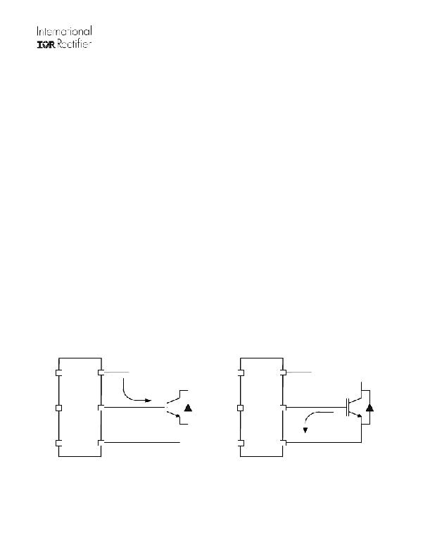
The IRS2336xD HVICs are designed to drive up to six MOSFET or IGBT power devices. Figures 1 and 2 illustrate
several parameters associated with the gate drive functionality of the HVIC. The output current of the HVIC, used to
drive the gate of the power switch, is defined as I O . The voltage that drives the gate of the external power switch is
defined as V HO for the high-side power switch and V LO for the low-side power switch; this parameter is sometimes
generically called V OUT and in this case does not differentiate between the high-side or low-side output voltage.
V B
(or V CC )
HO
I O+
V B
(or V CC )
HO
(or LO)
V S
+
V HO (or V LO )
-
(or LO)
V S
I O-
(or COM)
Figure 1: HVIC sourcing current
www.irf.com
18
(or COM)
Figure 2: HVIC sinking current
? 2009 International Rectifier
发布紧急采购,3分钟左右您将得到回复。
相关PDF资料
IRPLLED1A
IC MOSFET DRIVER
IRPLLED7
IC MOSFET DRIVER
IRPP3637-06A
BOARD REF DESIGN POWIR+
IRS2001MPBF
IC DRIVER HIGH/LOW SIDE 16MLPQ
IRS2001SPBF
IC DRIVER HI/LO SIDE 200V 8-SOIC
IRS2003STRPBF
IC DRIVER HALF-BRIDGE 8-SOIC
IRS2004PBF
IC DRIVER HALF-BRIDGE 8-DIP
IRS2011PBF
IC DRIVER HI/LO SIDE 8-PDIP
相关代理商/技术参数
IRMD26310DJ
功能描述:电源管理IC开发工具 COMPLETE 3-PHASE AC IRS26310DJ REF Kit RoHS:否 制造商:Maxim Integrated 产品:Evaluation Kits 类型:Battery Management 工具用于评估:MAX17710GB 输入电压: 输出电压:1.8 V
IRMDAC2
制造商:IRF 制造商全称:International Rectifier 功能描述:IR2133 Reference Design Kit: 3-Phase 230VAC 3HP Motor Drive 3-Phase 230VAC 3HP Motor Drive
IRMDAC3
制造商:IRF 制造商全称:International Rectifier 功能描述:Reference Design Kit: 3-Phase 460VAC 3HP Motor Drive
IRMDSS1
功能描述:KIT DESIGN IC REF SOFT START RoHS:否 类别:编程器,开发系统 >> 过时/停产零件编号 系列:- 标准包装:1 系列:- 类型:MCU 适用于相关产品:Freescale MC68HC908LJ/LK(80-QFP ZIF 插口) 所含物品:面板、缆线、软件、数据表和用户手册 其它名称:520-1035
IRMFB-EK
功能描述:光学传感器开发工具 Si1140 Multifunction Demo Board
RoHS:否 制造商:ams 工具用于评估: 接口类型: 最大工作温度:
IRM-H136/TR2
制造商:EVERLIGHT 制造商全称:Everlight Electronics Co., Ltd 功能描述:Infrared Remote-control Receiver Module
IRM-H136-TR2
制造商:EVERLIGHT 制造商全称:Everlight Electronics Co., Ltd 功能描述:Infrared Remote-control Receiver Module
IRM-H138/TR2
功能描述:红外接收机 Infrared Remote RoHS:否 制造商:Vishay Semiconductors 载频:20 kHz to 60 kHz 传输距离:5 m 显示角:+/- 50 deg 高电平脉冲宽度: 低电平脉冲宽度: 最小高电平输出电压: 输出电流:5 mA 工作电压:2.5 V to 5.5 V 电源电流:0.9 mA 功率耗散: 最大工作温度:+ 85 C 最小工作温度:- 25 C 封装 / 箱体: 封装:Reel